Product Summary
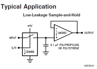
The LMC662CM CMOS Dual operational amplifier is ideal for operation from a single supply. It operates from +5V to +15V and features rail-to-rail output swing in addition to an input common-mode range that includes ground. Performance limitations that have plagued CMOS amplifiers in the past are not a problem with this design. Input VOS, drift, and broadband noise as well as voltage gain into realistic loads (2 kΩ and 600Ω) are all equal to or better than widely accepted bipolar equivalents.
Parametrics
Absolute maximum ratings: (1)Differential Input Voltage: ±Supply Voltage; (2)Supply Voltage (V+ -V-): 16V; (3)Output Short Circuit to V+ ; (4)Output Short Circuit to V-; (5)Lead Temperature (Soldering, 10 sec.): 260℃; (6)Storage Temp. Range: -65℃ to +150℃; (7)Voltage at Input/Output Pins: (V+) +0.3V, (V.) .0.3V; (8)Current at Output Pin: ±18 mA; (9)Current at Input Pin: ±5 mA; (10)Current at Power Supply Pin: 35 mA; (11)Junction Temperature: 150℃; (12)ESD Tolerance: 1000V.
Features
Features: (1)Rail-to-rail output swing; (2)Specified for 2 kΩ and 600Ω loads; (3)High voltage gain: 126 dB; (4)Low input offset voltage: 3 mV; (5)Low offset voltage drift: 1.3 μV/℃; (6)Ultra low input bias current: 2 fA; (7)Input common-mode range includes V; (8)Operating range from +5V to +15V supply; (9)ISS = 400 μA/amplifier; independent of V+; (10)Low distortion: 0.01% at 10 kHz; (11)Slew rate: 1.1 V/μs.
Diagrams

| Image | Part No | Mfg | Description |  |
Pricing (USD) |
Quantity | ||||||||||||
|---|---|---|---|---|---|---|---|---|---|---|---|---|---|---|---|---|---|---|
 |
 LMC662CM |
 National Semiconductor (TI) |
 Operational Amplifiers - Op Amps |
 Data Sheet |

|
|
||||||||||||
 |
 LMC662CM/NOPB |
 National Semiconductor (TI) |
 Operational Amplifiers - Op Amps CMOS DUAL OP AMP |
 Data Sheet |

|
|
||||||||||||
 |
 LMC662CMX/NOPB |
 National Semiconductor (TI) |
 Operational Amplifiers - Op Amps CMOS DUAL OP AMP |
 Data Sheet |

|
|
||||||||||||
 |
 LMC662CMX |
 National Semiconductor (TI) |
 Operational Amplifiers - Op Amps |
 Data Sheet |

|
|
||||||||||||
 (China (Mainland))


